


Hemeixin Electronics Co.,Ltd.
News
- Turn-key PCB AssemblyVarious processes are used to form a Turn-key PCB Assembly which includes Laser Ablation, Photoimaging, and plasma etching. The printed circuit material which uses HID designs always utilizes the organic reinforcement. These HDI layers are always built up to form the traditionally crated Multilayer Flexible PCB. They are built on the both sides o the traditional Microvia PCB which is done one by one with Microvias. Many choices can be made concerning the material and technology used in Microvias PCB. They can be filled with various equipment and processes. Metal Core printed circuit boards, abbreviated to MCPCB, or warm administration boards are printed circuit boards worked with a base Metal Core PCB used to scatter warm through the segments of the board, viably bringing down the core temperature of high warmth applications. They are utilized when customary fan-cooling procedures are deficient for cooling the whole framework.
2018 11/29
- Materials for making flexible circuit boardsFlexible Printed circuit board material one: insulating substrates The insulating substrate is a flexible insulating film. As the insulating carrier of the Circuit Board, selecting the flexible dielectric film requires a comprehensive investigation of the heat-resisting property, the coating performance, the thickness, the mechanical properties and the electrical properties of the material. Now commonly used in engineering is polyimide film, polyester commodity name Mylar) film and Polytetrafluoroethylene film. The general film thickness is selected within the range of 0.0127~0.127mm (0.5~5mil). Flexible Printed circuit board material two: adhesive chip The effect of the adhesive is to combine the film with a metal foil or an adhesive film and an overlay film.For different film substrates can be used different types of adhesives, such as polyester with a binder and polyimide adhesive sheet is not the same, polyimide substrate adhesive sheet epoxy and acrylic classification. The selection of the binder is mainly to investigate the fluidity of the material and its coefficient of thermal expansion. Non-bonded polyimide copper Foil Board, chemical resistance and electrical properties, etc. better. Due to the low glass temperature of the acrylic adhesive, the large amount of contamination in the drilling process is not easy to remove, affecting the quality of metallization hole, and other bonding materials, such as disappointments, so, Multilayer Flexible Crcuit interlayer adhesive commonly used polyimide material, because with the polyimide substrate, its Q CTE (thermal expansion coefficient) consistent, The problem of dimensional instability in multilayer flexible circuits is overcome, and other performances are satisfactory. Flexible Printed circuit board material three: copper foil Copper foil is a conductive layer covering the insulating substrate, which is then selectively etched to form a conducting line. The majority of this copper foil is made of rolled copper foil or electrolytic copper foil. The ductility and flexural resistance of the rolled copper foil are better than that of electrolytic copper foil, the elongation of the rolled copper foil is 20%~45%, and the elongation of electrolytic copper foil is 4%~40%. Copper foil thickness is most commonly used 35um (1oz), also has a thin 18um (o.5oz) or thick 70um (2oz), or even 105um (30z). Electrolytic copper foil is formed by electroplating, the crystalline state of copper particles is a vertical needle, easy to form a vertical line at the edge of etching, is conducive to the production of precision lines; however, the needle-like structure is prone to fracture when the bending radius is less than 5mm or dynamic deflection. Therefore, the flexible circuit base material uses the rolling copper foil, its copper particle is, can adapt to many times around the curve.
2018 11/26
- SMT PCB AssemblyThe process of surface mount SMT PCB assembly service can be simplified to a single panel: solder paste on the mounting and plug pads; SMC/SMD placement; TMC/TMD insertion; reflow soldering. Double panel: Solder paste-reflow soldering process to complete soldering of double-sided chip components; then solder paste on the B-side via component pads; reverse PCB and insert via components; third reflow weld. Prototype PCB Assembly One of the most popular technologies and processes in the electronics assembly industry today. It is a type of leadless or short lead surface mount component (referred to as SMC/SMD, Chinese called chip component) mounted on the surface of a printed circuit board (PCB) or other substrate surface. Circuit mounting technology for soldering and assembly by means of reflow soldering or dip soldering. Flexible Circuits Assembly has the advantages of reducing the assembly size and weight of the electronic product, avoiding wiring errors, increasing the flexibility of the organization, improving the reliability, realizing the three-dimensional assembly under different assembly conditions, saving the internal space of the product, reducing the volume of the finished product, and improving the performance of the product. Etc. Flexible Circuits Assembly with various advantages is relatively high in cost cost compared with other products, and has many production processes, high production difficulty, low yield and long production cycle.
2018 11/22
- Classification of rigid PCBhere are a variety of Classification methods for copper clad laminates. The general Classification method of the reinforcing material according to the plate, can be divided into: paper, glass fiber cloth, composite base (CEM series), multilayer laminates, special material base (ceramic, metal core base, such as our commonly used aluminum substrate is a special material base) five major categories. According to the characteristics of the CCL classification of Flame retardancy, can be divided into flame-retardant (UL94-VO, UL94-V1 grade) and non-flame-retardant (UL94-HB) two types of board. If the resin adhesive used by the plate is classified in different ways, common are: paper-based CCI, glass fiber cloth CCL and other special resins. Paper-based CCI, including phenolic resins, namely XPC, XXXPC, FR-1, FR-2, etc., in addition to epoxy resin (FE-3), polyester resin and other types. Fiberglass cloth CCL, including epoxy (FR-4, FR-5), is the most widely used type of fiberglass cloth today. Other specific resins, these specific resin plates are usually made of glass fiber cloth, polyimide fiber, non-woven fabric, etc. for the addition of materials, such as double maleimide modified triazine resin (BT), polyimide resin (PI), diphenyl ether resin (PPO), maleic anhydride-styrene resin (MS), polyisocyanate resin , Polyolefin resin and so on.
2018 11/19
- Circuit Board AssemblyPCB Welding Electrostatic Protection method: circuit board welding equipment must be grounded well, the workshop to maintain constant temperature, humidity environment. Should be equipped with anti-static material box, turnover box, PCB frame, anti-static wrist strap and other facilities. The static safety zone is 23±3℃ at room temperature and the relative humidity is 45-70%rh. It is forbidden to operate the electrostatic sensitive element in less than 30% of the environment. Non-production items such as tableware, tea sets, handbags, woolen fabrics, newspapers, rubber gloves, etc. are prohibited on the work Bench of the electrostatic safety zone. The worker enters the work area to be discharged. The operator must wear work clothes and no textile gloves on hand. Wear an antistatic wrist strap during operation and measure the wrist strap every day for effectiveness. Hair should not be scattered and must be jammed with a card. When mounting electrostatic sensitive devices, you should take one piece from the box, tube, and plate, and do not pile it on the table, nor fall off to the ground. Warehouse relative Humidity: 30-40%rh. Board processing process may not be arbitrarily stacked, all shelves. Here are some common precautions. Using multilayer PCBs as much as possible, the ground plane and the power plane, and the tightly spaced signal line-ground spacing can reduce common-mode impedance and inductive coupling to 1/10 to 1/100 of the duplex PCB, relative to the duplex PCB. Try to keep each signal layer close to a power layer or ground layer. For high-density PCBs with components on both the top and bottom surfaces, with very short connectors, and many fill floors, consider using inner lines. For double-sided PCBs, a tightly interwoven power supply and ground grid are used. The power cord is close to the ground and is connected as much as possible between the vertical and horizontal lines or the fill area. One side of the grid PCB copy board size is less than or equal to 60mm, if possible, the grid size should be less than 13mm. Make sure every circuit PCB copy board is as compact as possible. Put all connectors on one side as much as possible. If possible, introduce the power PCB copy board line from the center of the card and away from areas that are prone to direct ESD impact.
2018 11/16
- An Insight of the Flex PCB ManufacturingSuper High-end flex PCB, especially individuals for military programs, are produced with polyimide films simply because they provide the best efficiency. Aramid non-woven fiber material isn't pricey and has a great mechanical and electrical property. The main problem is that this material will absorb moisture. Fluorocarbons is a costly material as well as tough to handle. Nevertheless, it provides the best dielectric qualities. These components mostly use for controlled impedance programs. Most of these methods are used to provide a protective coating to these copper connectors in flex PCB manufacturing. Amongst these, the organic coating method has been used since the last many years. But unfortunately, this method is not without its share of disadvantages. It is not suitable for long-term usage, as it can cause erratic deviation in solder ability.
2018 10/19
- Microvia PCBThe microvia PCB type is a flexible and inflexible PCB combination that you could be looking for. These circuits are used in military space and aerospace applications, where a very dense circuit is needed. The rigid-flexible PCB helps a substantial amount of space, resulting in electronic items that measure much less. The term buried vertical interconnect access is those that are not visible from the exterior of the fabricated circuit board, and are formed in a sub-composite or copper-coated laminate. The vertical blind interconnects access those that are visible on the outside of the PCB, however, do not entirely pass through the board. By using the size of these small vertical interconnection ports, this interconnection density increases significantly on board. The Microvia printed circuit board uses these technologies to improve circuit density; For example, a cell phone that is using microvia technology due to the request of smaller packaging devices. Procedures used to shape microvessels include laser ablation, plasma etching, and photographic imaging.
2018 10/17
- HDI PCB: Defination, Features And Its Amazing BenefitHDI PCBs take some advantages of the latest existing technologies to amplify the circuit boards functionality using the similar or even little amounts of area. Such technological development in a board is motivated by the parts tininess as well as semiconductor packages which help superior characteristics in new innovative products such as touch screen tabs. Now, HDI PCBs are usually described by its high-density features consisting of high-performance materials, laser micro-vias, and fine lines. Its better density permits additional functions per unit area. Such forms of multifaceted structures provide the needed routing resolution for big pin-count chips that are utilized in high technology products and mobile devices. The placement of its parts on the circuit board requires extra precision compared to conservative board design because of miniature pads as well as the fine pitch of its circuitry on the circuit board. Also, leadless chips need special soldering ways and extra steps in the repair and assembly process.
2018 10/15
- thick copper pcbThick copper pcb is not a new innovation, as it has been used for a long time in PCBs that can withstand the exacting requirements of military and defense applications, such as in weapons controls. Mainstream electronics makers increasingly require ways to transfer heat away from components, and Thick copper pcb is becoming more prevalent in an growing number of non-military uses. Thick copper pcb boards are fabricated using plating and etching techniques. The goal is to add copper thickness to via sidewalls and plated holes. Plated holes can weaken if a board is subjected to multiple cycles while in production, and the addition of thick copper can strengthen these holes. Thick copper pcb boards structured with thick copper will allow for high current/power and control circuits on one Thick copper pcb board.
2018 10/12
- HDI PCB: Defination, Features And Its Amazing BenefitThere are so many innumerable advantages related to HDI PCB, like the small size, high speed, and high frequency. It's the main part of personal computers, portable computers, and mobile phones. Presently, HDI PCB is highly used in another end-user item that is, like game consoles and MP3 players, and so on. HDI PCBs take some advantages of the latest existing technologies to amplify the circuit boards functionality using the similar or even little amounts of area. Such technological development in a board is motivated by the parts tininess as well as semiconductor packages which help superior characteristics in new innovative products such as touch screen tabs.
2018 10/10
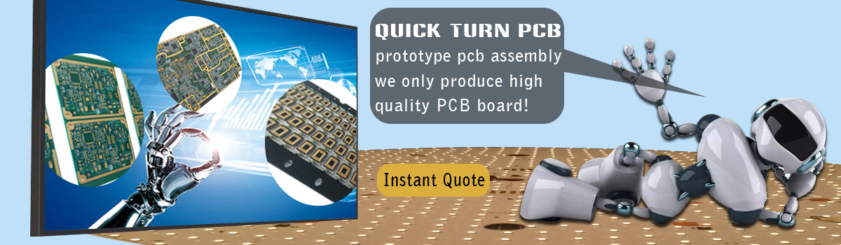
- PCB prototypeWe specialize in Quick turn PCB services with an industry leading turnaround time as fast as 72 hours.Not only do we know the importance of ensuring quick turnaround for the success of your project, but we also know that the resulting quality is equally as important. With our integrated in-house facility, 687-strong workforce, 87-plus dedicated engineer, 42 different PCB processing stations, and 24/5 production schedule, we can fulfill all PCB prototype projects on tight deadlines faster than the average lead times most PCB service companies can achieve - and with quality, of course. This means the shortest turnaround times and the highest quality for any HDI PCB project as well. Our current production capacity, which is 80,000 sq-ft of high quality and reliable PCBs, can meet customers' requirements for single to 50-layer boards in the shortest possible time. At our facility, the more layers required, the lesser time we need compared to the average. When your company needs fast and rapid PCB prototyping, know that you can count on Hemeixin to deliver high quality printed circuit boards on time at competitive prices. We have an industry leading on-time percentage that customers have come to love. We understand the importance of delivering on our promises, so we have a rock solid customer satisfaction guarantee.
2018 10/08
- Quick turn PCBThe attached photo shows an example of a fabricated QTA PCB. This is a 36 layer board with impedance control, gold surface finish, a 30:1 aspect ratio, depth controlled back drilling and pattern plating and was supplied in prototype quantities. Once the prototype board is evaluated and approved by the customer, HemeixinPCB can seamlessly switch to production quantities, since its QTA line is a mirror image of the tools and processes employed in the standard fabrication line, which is widely recognized for producing outstanding PCB quality. In addition, the staff at HemeixinPCB can offer expertise in design for manufacturability and process optimization for improving yields and product reliability.
2018 10/05
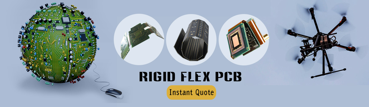
- rigid flex circuitsA rigid-flex design does not have a consistent set of layers across the entire circuit design, the rigid section of the board will have a different set of layers from the flexible section. And if the rigid-flex design has a number of rigid sections joined by a number of flex sections, then there may be a different set of layers used in each of these sections. A PCB editor with a single layer stack cannot support this design requirement. To support this, In rigid-flex packaging, a flexible circuit substrate provides a backbone of wiring with rigid multiplayer circuit sections built-up as modules where needed., as shown below. When to use rigid flex circuit board ? It`s getting harder to fit everything in the box; it`s also getting more costly. One solution promising to help designers meet the size constraint head on is rigid-flex PCB technology, but most design teams try to avoid using rigid-flex PCBs when product cost is an issue. But is it really as expensive as we think?
2018 10/03
- Flexible circuit BendingSpecial design for manufacturing (DFM) software tools for flex circuits help neutralize production problems during the design stage. These advanced tools are used to fully automate manual editing sessions, reducing errors and critical cycle time. Among today`s available flex DFMs are automatic joint curving and surface smoothing, and automated coverlay and solder mask optimization that make design faster, higher quality, and more accurate. its eliminate these joints, making them much more reliable and able to deliver overall higher product quality and longevity. So while rigid-flex PCB technology is certainly not new, various considerations now make it much more viable – not the least of which is cost.
2018 10/01
- thermal conductive MCPCBhis highly thermal conductive MCPCB is comprised of a regular aluminum core PCB and a specially embedded Copper Via that effectively draws the heat from the elements bonded on the top surface and distributes it to the aluminum core of the MCPCB. This innovation enables circuit engineers to have much less thermal restriction in circuit design and it offers more flexibility in components selection This unique and cost effective process developed by Cofan USA to embed Copper Via onto the Aluminum Core is completely contamination-free, and it makes it possible to integrate into conventional Aluminum Core PCB manufacturing processes. As a result, the MCPCB`s thermal conductivity is further enhanced through the Copper Vias, with no increase in cost. The cost is the same as an Aluminum Core PCBs which is relatively much lower than that of Copper Vias on Copper Core PCB. This Copper Via embedded Aluminum Core PCB is currently available for order, and ready for market consumption as with the conventional MCPCB with Copper Vias on Copper Core.
2018 09/28
- Heavy copper circuitsWhen it comes to developing the pieces of hardware, the process is not so simple. And, when it comes to printed circuit board (PCB) development efforts, the process becomes even more challenging. That's because PCBs are the launching points for hardware product development and the laminate and prepreg materials used in designing and manufacturing PCBs are the nuclei for those boards. (Prepreg is fiberglass cloth that has been saturated with resin that is not fully cured. As a PCB is placed under the heat and pressure of lamination this resin melts and flows into the voids in the adjacent copper layers filling them.) Semiconductor chip technology has become so advanced that testing these highly complex devices must be performed effectively to ensure high reliability and functionality. This allows chipmakers to convey to their OEM customers their highest confidences that their products are of the foremost quality and have been verified to operate according to their specifications. An automatic test equipment printed circuit board, or ATE PCB -- serving as an interface to a large test system -- is at the heart of all major test activities to verify a specific chip's functionality.
2018 09/26
- PCB Assembly and PCB FabricationATE PCBs are designed and assembled to test an array of different semiconductor chips, including microprocessors (µPs), memory, system-on-a-chip (SoC), field-programmable gate arrays (FPGAs), and others. However, an ATE PCB is designed and assembled specifically to test one particular kind of chip set. Some of today's highly advanced chips bring tens of millions of dollars into a chipmaker's coffers. In order to achieve that highly-prized chip-testing quality for chipmakers, a group of experienced program and project managers and highly-trained and savvy engineering personnel in ATE PCB assembly are of paramount importance. The requirements for disciplined administration management and assembly line technical knowhow are above and beyond that required for conventional PCB assembly. Considerable monetary loss and lost time-to-market are incurred if there's a misstep along the way toward successful assembly completion of an ATE PCB.
2018 09/24
- Turn Key PCB AssemblyQuick Turn PCBA Prototype and NPI builds are mission-critical to the speed up "Time-to-Market" and the success of your company`s new product introduction, and it is crucial to have a competent and trustworthy EMS partner. Try us, and you will find that Hemeixinpcb can far exceed both other EMS vendors performance and your expectations. Many of our customers have, with great satisfaction, transferred their PCB assembly operations to us from top tier electronic contract manufacturing providers, who frequently fail to provide priority attention, quality and responsiveness to any except their top-volume customers. Through the entire PCBA prototype and NPI process, Hemeixinpcb has consistently provided on-time deliveries that exceed our customers' quality, speed, and service expectations. We frequently receive customer appreciations for our level of quality and service in helping then launching new products swiftly to market at lowest total cost. Full Turn Key PCB Assembly
2018 09/21
- Full Turn Key PCB AssemblyThe production of the prototype is usually a prolonged process, but we assure you that we will also do this work speedily. You will observe that the production of yours turn-key PCB assembly is speedy and efficient. We are offering this service at very economical costs, and your product will assemble and ship to you instantly after the completion and tested by our quality control department. When your design is perfect, and you are happy with prototype, then we will produce a huge quantity in bulk. You can contact us at any time. We have adopted flexibility to provide prototyping services with full or partial turnkey pcb assembly wherein the components and all the inputs needed in the PCB assembly manufacturing as per the specifications in the BOM and Gerber File are being arranged by us fully or partially. One of the in house PCB prototype marvels, Hemeixinpcb facilitates PCB assembly services with no fuss, simple and fast prototyping with a unique way of using advanced techniques like automated design analysis, algorithms and custom technical specimens depending on the Gerber file and BOM ( Bill of Materials ) required for a particular prototype.
2018 09/19
- Complete Turnkey PCB AssemblyThere are many advantages if you will receive our services because many other people will not meet the deadlines which you assigned them. But we will fulfill every deadline and instructions ordered by you. You just have to put your design, and you will be notified on the spot about the quote of your design and the time duration of completion of turn-key PCB assembly work. We developed a complete system by using which you can easily observe the current status of your project and how much time will require more you can quickly judge it.
2018 09/17
Email to this supplier